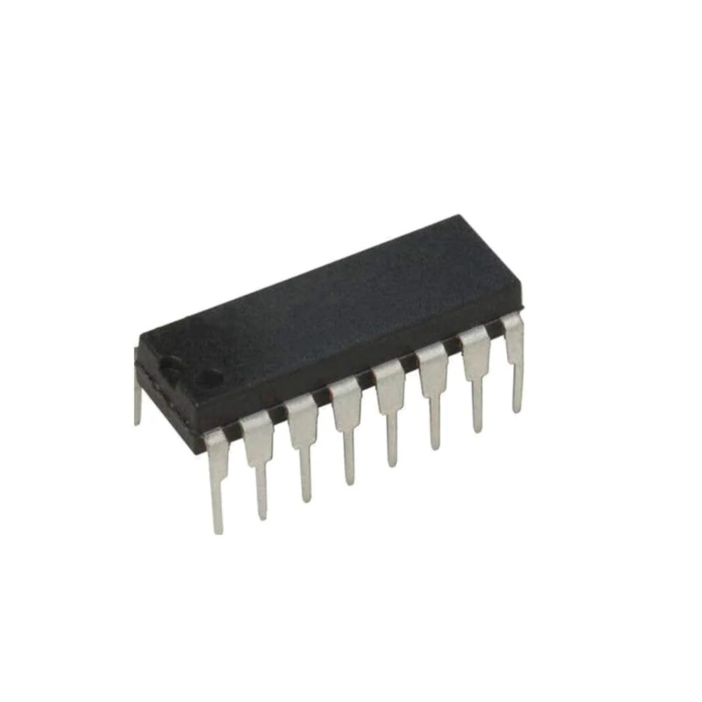
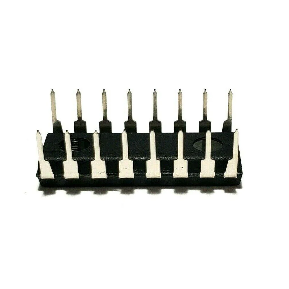
CD4042 Quad Clocked D Latch IC DIP-16 Package
CD4042 consists of four clocked ‘‘D’’ latches, designed by using monolithic complementary MOS (CMOS) technology, integrated with P- and N-channel enhancement mode transistors. For polarity e 0; the information present at the data input is transferred to Q and Q during 0 clock level; and for polarity e 1, the transfer occurs during the 1 clock level.
Technical Specification:
- Supply Voltage Range: 3 to 20V
- Input Current: ±10mA
- Power Dissipation: 200mW
- Low level Output Voltage: 0.05V
- High level Output Voltage Min.: 4.95V
- Low level Input Voltage Max.: 1.5V
- High level Input Voltage Min.: 3.5V
- Propagation Delay Time Max.: 500ns
Features:
- Clock polarity control
- Fully buffered data inputs
- Q and Q outputs
Applications:
- Bounce elimination switch
- Buffer Storage
- Data transfer
- Holding Register
- General Digital Logic
Product Information
Product Information
Shipping & Returns
Shipping & Returns


CD4042 Quad Clocked D Latch IC DIP-16 Package
CD4042 Quad Clocked D Latch IC DIP-16 Package
CD4042 consists of four clocked ‘‘D’’ latches, designed by using monolithic complementary MOS (CMOS) technology, integrated with P- and N-channel enhancement mode transistors. For polarity e 0; the information present at the data input is transferred to Q and Q during 0 clock level; and for polarity e 1, the transfer occurs during the 1 clock level.
Technical Specification:
- Supply Voltage Range: 3 to 20V
- Input Current: ±10mA
- Power Dissipation: 200mW
- Low level Output Voltage: 0.05V
- High level Output Voltage Min.: 4.95V
- Low level Input Voltage Max.: 1.5V
- High level Input Voltage Min.: 3.5V
- Propagation Delay Time Max.: 500ns
Features:
- Clock polarity control
- Fully buffered data inputs
- Q and Q outputs
Applications:
- Bounce elimination switch
- Buffer Storage
- Data transfer
- Holding Register
- General Digital Logic
Original: $0.35
-71%$0.35
$0.10Product Information
Product Information
Shipping & Returns
Shipping & Returns
Description
CD4042 consists of four clocked ‘‘D’’ latches, designed by using monolithic complementary MOS (CMOS) technology, integrated with P- and N-channel enhancement mode transistors. For polarity e 0; the information present at the data input is transferred to Q and Q during 0 clock level; and for polarity e 1, the transfer occurs during the 1 clock level.
Technical Specification:
- Supply Voltage Range: 3 to 20V
- Input Current: ±10mA
- Power Dissipation: 200mW
- Low level Output Voltage: 0.05V
- High level Output Voltage Min.: 4.95V
- Low level Input Voltage Max.: 1.5V
- High level Input Voltage Min.: 3.5V
- Propagation Delay Time Max.: 500ns
Features:
- Clock polarity control
- Fully buffered data inputs
- Q and Q outputs
Applications:
- Bounce elimination switch
- Buffer Storage
- Data transfer
- Holding Register
- General Digital Logic